
With the continuous development of nanotechnology, nano metal ultrafine powders have been increasingly widely used. However, during storage and transportation, nano metal ultrafine powders also face some problems, such as poor thermal stability and easy oxidation and heating. Therefore, we must take some measures to ensure the safe storage and transportation of nano metal ultrafine powders.
In order to ensure the stability of nano metal ultrafine powders, effective passivation measures must be taken during storage and transportation. Normally, we can achieve passivation treatment by inflating inert gas. Specifically, we can slowly fill the device with inert gas containing a small amount of air (about 1%) to maintain a stable oxide film thickness on the powder surface. During the inflation process, the selection of inflation speed, inflation amount, and passivation time is also crucial. It is necessary to flexibly adjust according to different powder characteristics to achieve the best passivation effect.
At the same time, we also need to pay attention to some details during the storage and transportation of nano metal ultrafine powders. For example, in storage containers, they must be kept sealed and placed in a dark, low humidity, well ventilated area to avoid moisture, heat, and direct sunlight. During transportation, it is necessary to strengthen vibration protection to prevent powder agglomeration caused by vibration, which can affect its performance.
In summary, the storage and transportation of nano metal ultrafine powders is a complex and rigorous process that requires us to fully understand the characteristics of nano metal ultrafine powders and take corresponding safety measures to ensure the safe storage and transportation of nano metal ultrafine powders.
How to understand the properties, synthesis, and applications of graphene quantum dots powder
Graphene quantum dots (GQDs) refer to a new type of carbon based fluorescent material with a graphene layer size of less than 100nm and a number of layers of less than 10. Generally speaking, graphene quantum dots include a large class of carbon fluorescent materials and their derivatives with similar structures and properties, including graphene quantum dots, oxidized graphene quantum dots, and partially reduced oxidized graphene quantum dots.
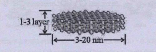
The Properties of Graphene Quantum Dots
UV absorption performance of graphene quantum dots
Due to the C=C double bond structure in graphene quantum dots, π - π transitions can occur, allowing them to absorb a large number of photons in a short wavelength range. Generally speaking, a strong absorption peak is displayed in the range of 260-320nm in the UV absorption spectrum, accompanied by a tailing that extends to the visible light range. Meanwhile, due to the influence of n - π transitions, graphene quantum dots may also exhibit shoulder peaks in the range of 270-390nm. Moreover, due to the influence of surface modification functional groups and surface passivation, the position and shape of the UV absorption peak will be affected.
Photoluminescence properties of graphene quantum dots
The luminescence performance of graphene quantum dots is its most important performance, and it is also the most widely studied and practical performance by researchers. Compared to spherical carbon quantum dots, graphene quantum dots with a layered structure have a more regular crystalline structure, resulting in higher fluorescence quantum yields.
Synthesis of Graphene Quantum Dots
There are two methods for preparing graphene quantum dots: top-down and bottom-up.
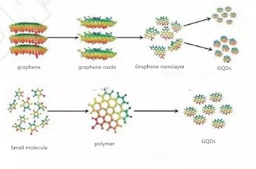
Top-down synthesis
The top-down approach refers to the physical or chemical etching of large-sized materials into nanoscale graphene quantum dots, which can be prepared through solvent thermal, electrochemical, and chemical exfoliation pathways.
The solvent thermal method is one of the many methods for preparing graphene quantum dots, and its process can be divided into three steps: first, the oxidized graphene is reduced to graphene nanosheets under high temperature in a vacuum state; Oxidize and cut graphene nanosheets in concentrated sulfuric acid and concentrated nitric acid; Finally, the oxidized graphene nanosheets are reduced in a solvent thermal environment to form graphene quantum dots.
The process of electrochemical preparation of graphene quantum dots can be summarized into three stages: the stage is the induction period when graphite is about to peel off and form graphene, and the color of the electrolyte begins to change from colorless to yellow and then to dark brown; The second stage is a significant expansion of graphite in the anode; The third stage is when the graphite flakes have peeled off from the anode and formed a black solution together with the electrolyte. In the second and third stages, sediment was found at the bottom of the beaker. In electrochemical reactions, there is an interaction between water and anions in ionic liquids, so the shape and size distribution of the products can be adjusted by changing the ratio of water to ionic liquids. The size of quantum dots prepared from electrolytes with high ion concentration is larger than that of electrolytes with low concentration.
The principle of chemical exfoliation of carbon fibers is to exfoliate the carbon source layer by layer through chemical reactions to obtain graphene quantum dots. Peng et al. used resin based carbon fibers as the carbon source, and then peeled off the graphite stacked in the fibers through acid treatment. Graphene quantum dots can be obtained in just one step, but their particle sizes are uneven.
Bottom up synthesis
The bottom-up approach refers to the preparation of graphene quantum dots using smaller structural units as precursors through a series of interaction forces, mainly through preparation pathways such as solution chemistry, ultrasound, and microwave methods.
The solution chemistry method is mainly used to prepare graphene quantum dots through the solution phase chemistry method of aryl oxidation condensation. The synthesis process involves the gradual condensation reaction of small molecule (3-iodo-4-bromoaniline or other benzene derivatives) polymers to obtain polystyrene dendritic precursors, followed by oxidation reaction to obtain graphene groups, and finally etching to obtain graphene quantum dots.
The microwave principle uses sugars (such as glucose, fructose, etc.) as carbon sources, because after dehydration, sugars can form C=C, which can form the basic skeleton unit of graphene quantum dots. The hydrogen and oxygen elements in hydroxyl and carboxyl groups will be dehydrated and removed in a hydrothermal environment, while the remaining functional groups will still bind to the surface of graphene quantum dots. They exist as passive layers, which can make graphene quantum dots have good water solubility and fluorescence properties.
The practical application of GQDs
Graphene quantum dots have important potential applications in fields such as biology, medicine, and new semiconductor devices. It can achieve single molecule sensors, and may also give rise to ultra small transistors or on-chip communication using semiconductor lasers for the production of chemical sensors, solar cells, medical imaging devices, or nanoscale circuits, among others.
Introduction to single crystal, polycrystalline, and amorphous nanomaterials
With the development of nanotechnology, single crystal, polycrystalline, and amorphous nanomaterials have become research hotspots. These nanomaterials have different structures and properties, and have a wide range of applications. Dongguan Saite New Materials focuses on the production and sales of powder materials such as nano metal powder, oxide powder, carbide powder, alloy powder, etc., and has become a leader in the nano material market.
1、 Single crystal nanomaterials
Single crystal refers to the arrangement of grains in a material in the same direction. Single crystal nanomaterials are essential materials for preparing high-performance electronic components, conductor materials, and optical materials due to their high purity and complete crystal structure. For example, single crystal nano gold powder has a wide range of applications and can be used in conductive slurries, solar cell electrodes, biosensors, and so on.
2、 Polycrystalline nanomaterials
Polycrystalline grains are arranged together in different directions, and polycrystalline nanomaterials have excellent properties in strength, toughness, corrosion resistance, and can be used in fields such as electronics and aerospace materials. Polycrystalline nano titanium oxide powder can be used as a catalyst, UV barrier, anti UV coating, and other applications, while polycrystalline nano silicon carbide powder can be widely used in abrasive, cutting, ceramics and other fields.
3、 Amorphous nanomaterials
Amorphous nanomaterials refer to crystalline forms in materials that are not clearly defined. Amorphous nanomaterials have shown broad application potential in potential fields, such as preparing efficient catalysts, biomedical imaging materials, etc. Because amorphous nanomaterials exist in practical materials such as glass and have advantages such as transparency, hardness, and smooth surface, they are used in the production of high-tech products such as mobile phone screens and solar cells.
In the field of materials science, single crystal and polycrystalline are two different types of crystal structures. There are significant differences in their crystal structure, physical properties, preparation methods, and application fields.
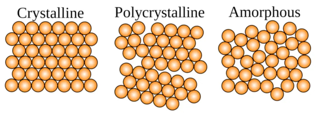
crystal structure
Single crystal refers to a crystal in which the lattice structure is complete, continuous, and orderly arranged, without grain boundaries or particle boundaries. This perfect crystalline structure enables single crystals to have higher crystallinity and crystal integrity. Polycrystalline materials are composed of many grains, which are connected to each other through grain boundaries. Grain boundaries are the interfaces between different grains within a crystal, where atoms or molecules are arranged relatively disorderly. Therefore, compared to single crystals, polycrystalline materials have a less perfect crystal structure, and the presence of grain boundaries also makes them heterogeneous and non-uniform.
physical property
Due to the highly ordered lattice structure of single crystals, their physical properties are usually more uniform and consistent than those of polycrystals. Single crystals exhibit good properties in electrical, optical, thermal, and mechanical fields, and possess isotropy (having the same properties in any direction). For example, monocrystalline silicon is widely used in semiconductor manufacturing for the production of integrated circuit chips due to its high conductivity, low conductor resistivity, and low leakage current. However, due to the presence of grain boundaries, polycrystalline silicon can lead to heterogeneity and non-uniformity in physical properties. For example, the resistivity and leakage current of polycrystalline silicon are usually higher than those of monocrystalline silicon.
Preparation method
The preparation process of single crystals usually requires precise control conditions and technical means, such as suspension method, vapor deposition method, floating zone method, etc. These methods can maintain a highly ordered lattice structure during the growth process of single crystals. The preparation of polycrystalline materials is relatively simple, often using methods such as melting and solidification. These methods can change the grain size and distribution by adjusting the preparation conditions, but the crystal structure of polycrystalline materials is often complex and difficult to control its lattice structure and growth direction.
application area
Due to its better physical properties and crystallinity, as well as the advantage of no grain boundaries, single crystals have a wide range of applications in certain specific fields. For example, in the field of optics, single crystal materials are used to produce high-precision optical lenses and laser devices. In addition, single crystal alloys are widely used in the aerospace industry to manufacture high-temperature structural components due to their high thermal stability and oxidation resistance. Polycrystalline materials, due to their simple preparation methods and low cost, are widely used in some basic material fields, such as steel manufacturing, ceramic manufacturing, etc.
In summary, there is a clear difference between single crystal and polycrystalline materials. Single crystals have a more perfect crystal structure and better physical properties, but their preparation is difficult and costly; The preparation of polycrystalline materials is relatively simple, but the crystal structure and physical properties are relatively complex and uneven. In terms of application fields, single crystals are widely used in some high-precision fields, while polycrystals have a wide range of applications in some basic materials fields.
Understanding Dry and Wet Techniques for Nanomaterial Preparation
Introduction:
Nanotechnology is becoming increasingly important in many fields, from medicine to electronics. Nanomaterials, including nanoparticles, nanotubes, and nanowires, are essential components of many nanotechnology applications. Producing these materials requires specialized techniques, such as wet and dry methods. In this article, we will explore what dry and wet methods are, their benefits, and how SAT NANO provides high-quality nanomaterials.

Dry and wet methods are two of the most common techniques for preparing nanomaterials. Dry methods refer to techniques that produce nanomaterials without the use of a solvent, while wet methods utilize a liquid medium.
Dry methods have several advantages over their wet counterparts. For instance, dry methods are simpler and less expensive since they do not require the use of a solvent. Moreover, dry methods produce a high yield of nanoparticles and are highly scalable, making them ideal for large-scale production.
On the other hand, wet techniques enable the production of high-quality nanomaterials with well-defined structures. They can also produce a wide range of nanomaterials, including complex and multifunctional particles. Wet methods are commonly used for the synthesis of nanomaterials in suspension, which have many important applications—for example, in medicine, where they can be used to deliver drugs directly to target cells in the body.
SAT NANO provides high-quality nanomaterials through a combination of dry and wet methods. Our team of experts selects the most appropriate method for each type of nanomaterial, depending on its intended application. We use state-of-the-art equipment to prepare nanomaterials to exacting standards. This ensures that our customers receive high-quality materials that meet their specific requirements.
Conclusion:
In conclusion, nanomaterials are essential components of many applications in a variety of fields. Dry and wet methods are two common techniques used in the preparation of nanomaterials. Dry methods are ideal for large-scale production, while wet methods excel in producing complex, well-defined nanomaterials. SAT NANO provides high-quality nanomaterials using a combination of these techniques, ensuring that our customers receive the best possible products for their needs.
What are the surface coating treatment methods for ultrafine powders
Ultrafine powder is one of the essential raw materials in many industrial production processes. Its advantages over traditional ordinary powder are smaller particle size, smoother surface, easier processing, and easier dispersion. To better utilize ultrafine powders, surface coating treatment is necessary to improve their quality and performance. This article will introduce several methods for surface coating treatment of ultrafine powders.
Method 1: Physical surface coating treatment
The commonly used methods for surface coating treatment using physical methods mainly include mechanical alloying, high-energy ball milling, vapor deposition, chemical vapor deposition, and physical deposition. Among these methods, especially the physical deposition method, it is one of the most commonly used surface coating treatment methods. The physical deposition method can change the properties of ultrafine powders by forming a layer of crystalline or amorphous films at the micron and submicron levels on their surface. This method can not only improve the stability of ultrafine powder, but also improve its flowability without damaging the original properties of ultrafine powder.
Method 2: Chemical surface coating treatment
Chemical surface coating treatment is a superfine powder surface coating material prepared by chemical methods. The commonly used chemical methods for surface coating treatment include solvent deposition, co precipitation, and double decomposition. Among them, solvent deposition is a common method. The principle of this method is to place surfactants on the surface of ultrafine powder to form a uniform film, which can improve the properties of ultrafine powder, such as color, stability, and dispersibility.
Method 3: Physicochemical surface coating treatment
The physicochemical surface coating treatment mainly combines chemical and physical methods to form a new material to coat the surface of ultrafine powder. The commonly used physicochemical methods for surface coating treatment include in-situ polymerization, electrodeposition, ion implantation, and plasma thin film deposition. These methods can improve the corrosion resistance, oxidation resistance, wear resistance, and enhance the conductivity of ultrafine powders.
In summary, there are various methods for surface coating treatment of ultrafine powder, and different methods can also make the characteristics of the treated ultrafine powder different. As a high-quality supplier, SAT NANO not only provides high-quality ultrafine powders, but also provides comprehensive services to customize surface coating treatment solutions for ultrafine powders suitable for different industries. Whether you are a pharmaceutical, chemical, or electronic enterprise, Saite can provide you with professional and high-quality products and services.
What are the surface modification methods for alumina powder
What are the surface modification methods for alumina powder?
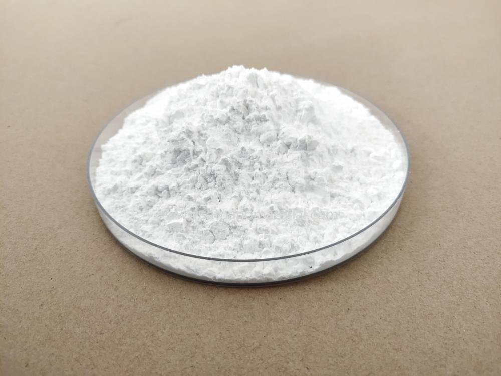
Aluminum oxide, a common material, is commonly used in the production of ceramics, coatings, catalysts, etc. However, in some applications, such as filling composite materials or preparing high-performance catalysts, surface modification of alumina is required to improve its performance and stability. This article will discuss the surface modification methods of alumina.
Surface modification is the process of introducing a certain substance (modifier) into the surface of another substance (material to be modified) to improve the properties and functions of the material. The commonly used processes for surface modification of alumina include chemical treatment, deposition, and other methods, among which the most common is the modification of alumina by silane coupling agent (KH-560).
Silane coupling agent (KH-560) is a versatile organic silicon compound with good surface affinity and reactive properties. It can react with the surface of alumina to form chemical bonds, thereby achieving stable surface modification. When using KH-560 for modification, attention should be paid to factors such as the amount added, pre hydrolysis pH value, pre hydrolysis time, reaction temperature, reaction time, and stirring rate to ensure the desired modification effect.
The specific modification method is to first prepare a solution with an alcohol water ratio of 1:8, add an appropriate amount of KH-560, stir evenly, and the amount of KH-560 should be KH-560: alcohol: water=20:9:72. Then use 40% acetic acid to adjust the pH value, pre hydrolyze it for 1 hour, reaction temperature is 60 ℃, and stirring rate is 1500r/min. After pre hydrolysis of KH-560, fully disperse micrometer sized Al2O3 in an appropriate amount of ethanol for about 1 hour. Slowly add a certain amount of KH-560 to the uniformly dispersed micrometer sized alumina for a mixing reaction. After the reaction is completed, filter and wash three times with ethanol. Dry at 60 ℃ for 3 hours to obtain the modified alumina material.
To verify the modification effect, various tests and characterizations such as oil absorption value, viscosity, SEM, and FTIR can be carried out. The experimental results showed that KH-560 was successfully grafted onto the surface of alumina powder, and the modified powder had smooth particle edges and no obvious agglomeration phenomenon. Meanwhile, the oil absorption value of the modified alumina powder decreased by 43.4%, and the viscosity decreased by about 16.1%. This indicates that the surface modification method of alumina can effectively improve its physical and chemical properties, thereby adapting to a wider range of application fields.
SAT NANO is one of the best supplier of Aluminum oxide nanopowder, we can supply 30-50nm, 100nm, if you have any requirement on alumina powder, please feel free to contact us at admin@satnano.com
What is the amount of thermal conductive nanomaterials added
With the continuous progress of technology, the application of thermal conductive nanomaterials in modern industry is becoming increasingly widespread. From electronic devices to the automotive industry, their use has become an industry standard in today's high-tech field. As a company specializing in the production of thermal conductive nanomaterials, Dongguan SAT NANO understands the importance and role of thermal conductive nanomaterials in industrial manufacturing. And an important question is: what is the amount of thermal conductive nanomaterials added?
Firstly, we need to understand the characteristics of thermal conductive nanomaterials. Due to its small particle size, thermal conductive nanomaterials can efficiently transfer heat energy. Compared to traditional thermal conductive materials, they can provide better thermal conductivity at relatively small amounts of addition. Therefore, the amount of thermal conductive nanomaterials added is usually very small, and only a small amount of material needs to be added to achieve a high thermal conductivity effect.
Different products require different amounts of additives. Based on our experience, the amount of thermal conductive materials added is usually based on the volume of the product. For electronic devices, in most cases, only a small amount of thermally conductive nanomaterials need to be added to achieve good thermal conductivity. For larger machinery and equipment, it may be necessary to add more thermal conductive materials.
Assuming the thermal conductivity of the target material is λ_ m. The thermal conductivity of thermal conductive powder is λ_ p. The formula for calculating the amount of thermal conductive powder added is: amount added (%)=( λ_ M- λ_ 0)/( λ_ P- λ_ 0) × Among them, λ_ 0 represents the thermal conductivity of the target material without the addition of thermal conductive powder.
In addition to the specifications and shape of the product, the application scenario is also another factor that needs to be considered. For example, products used in high-temperature environments require the addition of more thermal conductive materials to improve their heat resistance performance. Similarly, some devices that need to withstand high pressure also require more thermal conductive materials to maintain their thermal conductivity.
In summary, the amount of thermal conductive nanomaterials added is determined based on different products and application scenarios. Dongguan Saite, as a professional manufacturer of thermal conductive materials, can provide customers with targeted production solutions to ensure that its products can have maximum efficiency in any situation.
As a customer of Dongguan SAT NANO, you can confidently use our thermal conductive nanomaterials to ensure that your products can perform well in the most challenging environments.
SAT NANO is one of best supplier of metal nanoparticle, oxide nanoparticle and carbide nanoparticle, if you have any enquiry, please feel free to contact us at admin@satnano.com
What is the correlation between PPM, PPB, and PPT in solution
With the continuous development of nanotechnology, nano powder dispersion, as an important nano material, has attracted more and more attention. SAT NANO, as a company specializing in the production of nano materials, provides high-quality nano powder dispersion. This article will introduce the conversion of PPM, PPB, and PPT in solutions and their respective meanings.
PPM stands for "Parts per million", which is one of the units representing the concentration of substances in a solution. It generally refers to the proportion of the weight of the dissolved substance to the total weight in a solution of one millionth. For example, if a solution contains 10 grams of substance A with a total weight of 1000000 grams, the concentration of substance A is 10 PPM.
Similar to PPM, PPB is also a unit of measurement that represents the mass of substances contained in every billion parts. Usually used in highly detailed chemical experiments, such as in experiments studying air pollution. The conversion rate of PPB is thousands of times that of PPM, which means 1 PPM=1000 PPB.
PPT stands for "Parts per trillion" (abbreviated as PPT), which is a very small proportion. PPT is usually used for extremely precise detection and represents a very high level of accuracy. PPT is used in many fields of environmental and scientific analysis, such as environmental pollution detection, food quality control, and drug production. The conversion between PPT and PPB is 1 PPB=1000 PPT.
Nano powder dispersion is an important nano material and has a broad application prospect. It can be used to prepare nanomaterials with diverse forms and can also be used to prepare nanomaterials with different physical and chemical properties. SAT NANO's nano powder dispersion has been carefully prepared to ensure its good dispersivity and high purity.
In actual production, understanding the conversion of PPM, PPB, and PPT and their respective meanings is very important. For the concentration analysis and control of chemical substances, we need to have a deep understanding of these units. SAT NANO will continue to provide customers with high-quality nano powder dispersion, and explore broader application prospects with customers.
SAT NANO is one of the best supplier of nano powder dispersion, we can offer al2o3 dispersion, ZnO dispersion, SiO2 dispersion and other many kinds of dispersion, if you have any enquiry, please free to contact us at admin@satnano.com
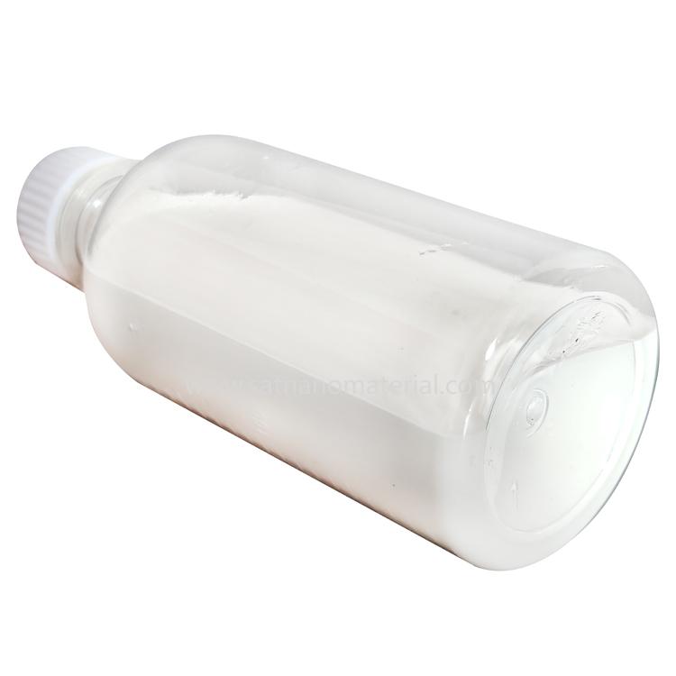
What is the role of the passivation layer of metal nanoparticles
Metal nanoparticles are a widely used material that can be applied in various fields, such as medicine, electronics, energy, and the environment. They have extremely small size and high surface area, which can enhance the performance of many materials. However, the surface of metal nanoparticles is often very active and easily reacts with the surrounding environment, so a passivation layer is needed to protect their surface. This article will explore the role of the passivation layer of metal nanoparticles.
The passivation layer is a thin film that covers the surface of metal nanoparticles, usually composed of inorganic or organic substances. This thin film can protect the surface of metal nanoparticles and prevent them from reacting with the surrounding environment. Especially in catalytic reactions, the surface of metal nanoparticles often reacts with reactants, and the passivation layer can prevent such reactions from occurring, thereby improving the selectivity and efficiency of the reaction.
In addition, the passivation layer can also affect the stability and dispersion of metal nanoparticles. Metal nanoparticles often gather together to form clusters in water, and the passivation layer can disperse and stabilize them, ensuring the stability and consistency of their performance.
As a company that provides high-quality metal nanoparticles, SAT NANO values the quality and stability of its products. After years of research and development, the company’s research team has successfully developed a unique passivation layer technology that can enhance the stability and activity of metal nanoparticles. At present, Saite’s metal nanoparticles have been widely used in multiple fields, such as medicine, electronics, and the environment.
In summary, the passivation layer of metal nanoparticles plays a crucial role in protecting their surface, improving reaction selectivity and efficiency, as well as maintaining stability and dispersion. As a professional supplier of metal nanoparticles, Saite continuously develops more advanced technologies for product manufacturing in different fields to meet the needs of customers.